OLED Distinctions
OLEDs vs. PLEDs
- Commonality: Both are organic light-emitting devices.
- Differences:
- OLEDs:
- Made from smaller organic molecules.
- Typically manufactured using vacuum evaporation techniques.
- PLEDs:
- Utilize polymers for their structure.
- Still primarily in the research phase.
- Potential for producing large, cheap, flexible displays.
- OLEDs:
AMOLED vs. PMOLED
- PMOLEDs:
- Consume more energy.
- Best suited for small screens.
- Simple and inexpensive to manufacture.
- AMOLEDs:
- Incorporate an additional layer of transistors.
- Offer faster refresh rates and lower power consumption.
- More challenging and costly to produce.
Bottom Emission vs. Top Emission vs. Transparent OLEDs
- Bottom Emission: Cathode is opaque; anode and substrate are transparent.
- Top Emission: Anode is opaque; cathode is transparent.
- Transparent OLEDs: Both the anode and cathode are transparent.
Generations of OLED Technology
- 1st Generation – Fluorescent OLEDs:
- Utilize only singlet exciton pairs.
- Maximum efficiency: 25%.
- 2nd Generation – Phosphorescent OLEDs:
- Exploit both singlet and triplet exciton pairs.
- Significantly higher efficiency compared to the first generation.
Physics of OLEDs
Traditional LED Operation
- Inject charges to fill holes and emit light.
Basic OLED Structure
- Most basic design includes three layers:
- Anode
- Cathode
- Active Layer
- Introduced around 1965.
- Process:
- Charge injection.
- Charge transport.
- Exciton formation.
- Radiative recombination.
Key Concepts
- Charge Speed: Charges must move quickly enough to form excitons before they recombine non-radiatively.
- Forward Bias: Light is emitted when the device is powered correctly.
- Reverse Bias: Occurs when the device is connected incorrectly, preventing light emission.
- Equilibrium: The device is not powered, and no light is emitted.
Electron Blocking Layer (EBL)
- Prevents excess electron migration, ensuring efficient recombination in the active layer.
Qualities of OLEDs
Luminous Efficiency
Where:
- : Driving voltage.
- : Current.
- Luminous flux.
Electroluminescence Quantum Efficiency
- Represents internal efficiency, ignoring photon transport losses.
Where:
- : Photoluminescence efficiency. Improved by suppressing non-radiative channels.
- : Ratio of singlet excitons to total excitons (max: 25%).
- : Exciton formation factor. Improved by balancing charge injection and transport.
Optimizing OLED Performance
Improving : Suppress Non-Radiative Decay Channels
- Prevent Aggregation Quenching:
- Avoid close packing of chromophores.
- Dilute active materials with a matrix substance.
- Design non-stacking chemical structures (e.g., polythiophenes, oligothiophenes).
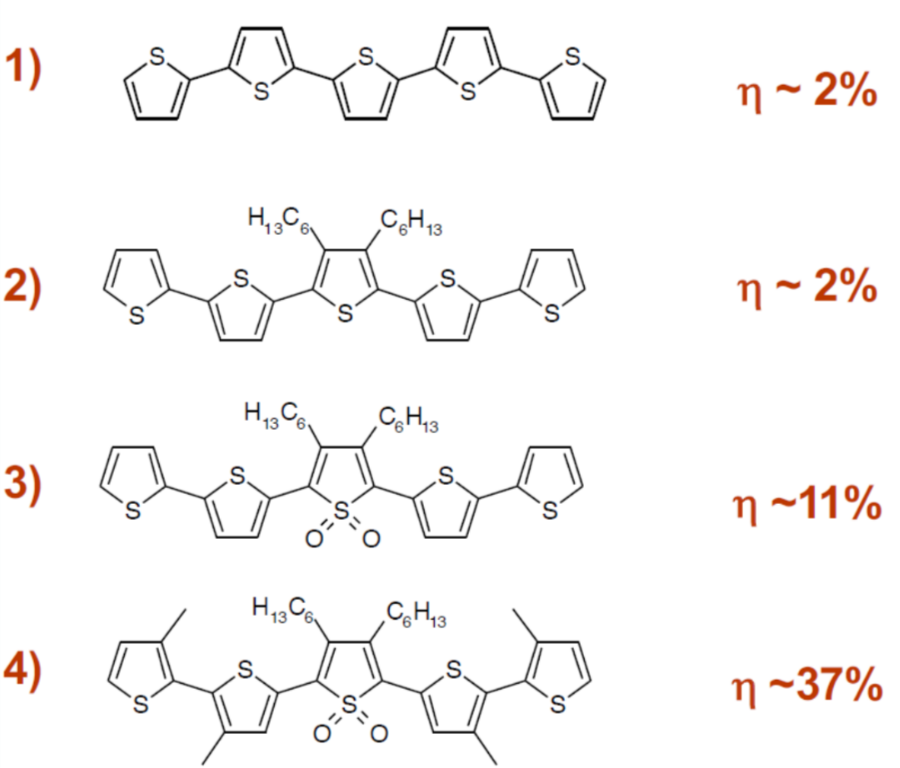
Oligothiophene efficiency increases
- Lower crystallinity improves efficiency.
- Optimize Optical Design:
- Minimize waveguiding, reabsorption, and refraction losses.
- Ensure charges recombine only in desired regions.
Increasing : Boost Radiative Excitons
- Max Efficiency: 25%.
Methods:
-
Triplet-Triplet Annihilation (TTA):
- Converts two triplets into a singlet.
- Theoretical efficiency: 62.5%.
- Practical efficiency: ~40%.
-
Thermally Activated Delayed Fluorescence (TADF):
- Reverse intersystem crossing (triplets to singlets).
- Requires complex, heavy molecules.
- Potential 100% efficiency.
-
Hybrid Local Charge Transfer (HLCT):
- Donor-acceptor molecules with similar singlet and triplet energies.
- Theoretical efficiency: 100%.
-
Harvesting Phosphorescence:
- Theoretical photoluminescence quantum yield (PLQY): 100%.
- Techniques: Foerster transfer, Dexter transfer, and E-H direct capture.
Challenges:
- Materials with low TTA.
- Blue emitters are challenging.
- Efficiency drop at high currents.
- Dexter transfer is slow due to its short range.
Improving : Enhance Charge Balance
-
Balancing Charge Injection:
- Cathode: Add alkaline materials to reduce work function.
- Anode: Modify ITO work function using:
- Self-assembled monolayers.
- Spin-coated layers.
- Layer-by-layer deposition of dedoped layers.
- Oxygen plasma treatment (standard method).
-
Balancing Charge Transport:
- Reduce excess majority carriers.
- Add separate electron and hole transporting layers.
- Form heterojunctions for efficient recombination.