Error Analysis and propagation for each theoretical period:
Section 2: Voltage divider
Objective:
Create and use a voltage divider for use in section 3, the Op-Amp circuit. Utilize previous circuits knowledge and analyze voltage divider theoretically and experimentally.
Equipment:
Resistors, Multimeter, Osciliscope, Jumper Cables, 555 Timer circuit from section 1, 9v battery and harness.
Procedure:
Perform calculations to determine theoretical voltage attenuation given certain resistors value. Target for voltage attenuation is 10x. Use breadboard, resistors, and jumpers to create circuit outlined in diagram below. Apply voltage and use multi-meter to verify the calculated voltage attenuation is accurate.
Beginning with the target attenuation (10x), we can calculate the ratio of resistance we need.
Rearrange to solve for attenuation
Rearrange this to solve for the required resistance
This is the required ratio between our two resistors.
Experimentally measured resistance of the resistors:
| | R1 | R2 |
|------------|------------|------------|
| Resistance | 19.89 +- 0.9% kohm | 2.189 +- 0.9% kohm |
Given these resistance values, we can calculate the theoretical voltage attenuation with the measured resistance.
Performing Error Propagation on the results:
Results
Above is the Oscilloscope reading for and , with on channel 1 and on channel 2. You can clearly see the attenuation, however, the scaling on channel 2 was increased relative to channel 1 to retain clarity. Measurements of with a steady power supply yielded an experimental of 0.951 volts, with a of 9.60 volts.
Analysis
Looking at these results, we can easily calculate the experimentally measured attenuation. With a of 9.60 and a of 0.951, gain is calculated by:
As seen here, the experimental value matched the theorized value for our measured resistances to the extent of the accuracy of our measuring equipment.
Conclusions:
This experiment verified that the experimentally measured attenuation matched the theoretically calculated attenuation to the highest accuracy we could measure with our lab equipment. We were not able to perfectly match our goal of 10x attenuation due to a lack of properly matched resistors.
Section 3
Objective:
The objective of this portion of the lab is to use an Operational amplifier, or Op-Amp integrated circuit to create an inverting amplifier and “reverse” the previous attenuation performed with the voltage divider and testing if the theoretically calculated amplification values are in line with the experimentally measured and verified values.
Equipment:
T-I Op-amp chip, breadboard, circuits from Section 1 and 2, oscilloscope, multi-meter, pair of resistors to yield desired gain and 9v power supply.
Procedure:
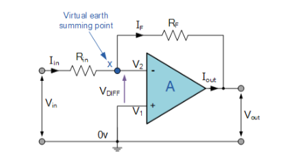
First begin by calculating the appropriate gain while taking care to ensure that the amplifier is not being pushed beyond its limits. Since section 2 yielded an attenuation of 10x, the operational amplifier circuit has to have a less then 10x gain. To achieve this, a pair of resistors has to follow the following relation:
Where and are labeled in the diagram below
After computing the theoretical gain from the resistors, we can proceed to compute the experimental gain. Using the oscilloscope or DMM to measure the gain produced from the inverting Op-Amp circuit.
Data
Picture of the Op-Amp circuit (Top IC) and 555 Timer circuit (Bottom IC)
!picture here!
Our measured resistor values:
| Resistance | 830 0.9% | 98.7 0.9% |
Using equation for inverting Op-Amp gain:
We can plug in our measured values to calculate gain and uncertainty in gain
Computed Gain:
Results with constant 9v signal:
Calculated gain and uncertainty from experimental voltage measurements
Experimental Gain
Conclusion:
The theoretical and experimental gain and uncertainty produced from the inverting Op-Amp correlated very closely, both within the uncertainties of each other. This evidence verifies the operation of the inverting Op-Amp circuit being regulated by the equations stated above.
Analytical Design Problem:
! Insert picture here
Given this non-inverting amplifier circuit, we need to find how to calculate the gain based on values of and . We can accomplish this using the golden rules:
- The voltage across and in series is equivalent to .
- Using the voltage divider equation we can find , the potential between and . In the below equation, is from the op-amp and is
- to the op-amp is always kept the same as due to golden rule #1. We can rewrite the above formula with these substitutions
- Rewrite to solve for
Section 4
Objective:
The objective of this section was to combine passive elements such as capacitors and inductors to create a low-pass frequency filter. This will build upon the previous sections, using the amplified signal from section 3 as an input.
Equipment:
Previously built circuits, capacitors, resistors, multi-meter, oscilloscope, jumper wires, 9v power supply.
Procedure:
To create and test this low pass filter, we need to combine a resistor and a capacitor in the diagram shown below:
 The problem gives us values to use for the capacitor and resistor, 47 and 4.7 respectively. We will first calculate the theoretical voltage attenuation at 100Hz and 10kHz. After performing these calculations, we next must experimentally verify them. However, we are not given a 47 capacitor, but we have 95 capacitors. We can combine 2 95 capacitors in series to achieve our desired capacitance.
Using these components and building the circuit, the next step is to connect the output of section 3 into the of the low pass filter. Next, we are to test the circuit with a 100Hz signal and a 10kHz signal. Finally, we will take measurements and compare this to our theoretical findings.
Data:
This above photo shows the rising and falling edges of the waveform. You can see how the square wave is separated and the lower frequency components are passed while the higher frequency components are attenuated out.
The above photo shows both the rising and falling edges, with a few wave cycles. This photo shows, in less detail, the attenuation of the higher frequency components of the square wave. This correlates with the diagrams presented in the lab instructions as well.
Conclusions:
The low pass filter functioned as expected, resulting in expected attenuation of higher frequency components of the square wave.