Semiconductivity in Organic materials (Carbon based, think plastic) emerges from hybridization of orbitals, and pi orbital conjugation. This gives rise to bound states such as polarons and excitons and effects such as phosphorescence.
| Advantages | Disadvantages |
|---|---|
| More flexible | Slower then silicon |
| Cheaper, easier to mfg. | Sensitive to UV, Water |
| Compatible with biological tissue | |
| Can be printed |
Background
- Organic Polymers and Molecules can become semi-conductive through SP2 orbital hybridization What does this mean?
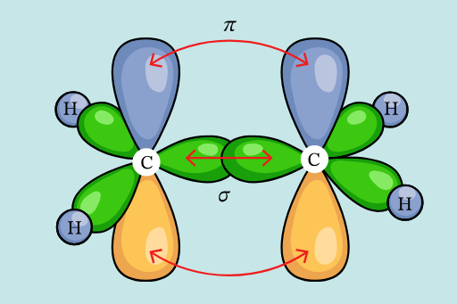
One s (sigma) orbital and 2 p (pi) orbitals combine to form an sp2 hyrbid orbital
Effects:
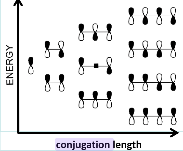
Conjugation: the delocalization of pi bonds over many carbon atoms. This leads to electrons being free to move throughout the material. The conjugation length represents the number of monomers over which the delocalization of electron occurs. A shorter conjugation length leads to a larger band gap and a blue-shift of the emission spectra.
LUMO and HOMO: Lowest unoccupied molecular orbital and highest occupied molecular orbital. Distance between these helps determine band gap.
Increasing conjugation length lets π-electrons delocalize more, which lowers the energy difference between HOMO and LUMO — shrinking the bandgap and improving optoelectronic performance.
Peierl’s Transition (dimerization)
- Alternating short and long bonds
- Different types, degenerate and non-degenerate dimerization. Degenerate as in having the same energy
Solitons
| Neutral | Positive | Negative | |
|---|---|---|---|
| Spin | +/- 1/2 | 0 | 0 |
| Charge | - |
- Oppositely charged Solitons will annihilate. Like Solitons will form a large separation-
Polarons:
- Polarons are a bound state that has both spin and charge
- Represents a structural deformation moving through a material
- Quasiparticle
The presence of more polarons will cause several effects in an OSC:
- Reduced charge mobility, reduction in conductivity
- Distorts the HOMO and LUMO levels, typically causing the band gap to functionally shrink
- Can exhibit thermal effects, causing resistance to go down as temp increases
- If polaron formation energy is high, it can act as an energy barrier in charge injection
Excitons
- Yet another Quasiparticle
- Bound state of a hole and an electron, doesn’t live long.
- Can recombine to form light
| Wannier Exciton | Frenkel Exciton |
|---|---|
| Weak electron hole coupling | Strong electron-hole coupling |
| Binding energy 10 meV | Binding energy 0.2-1 eV |
| Large distance (~10nm) | Small distance (~1nm) |
| Typical in inorg. semiconductors | Typical in OSCs |
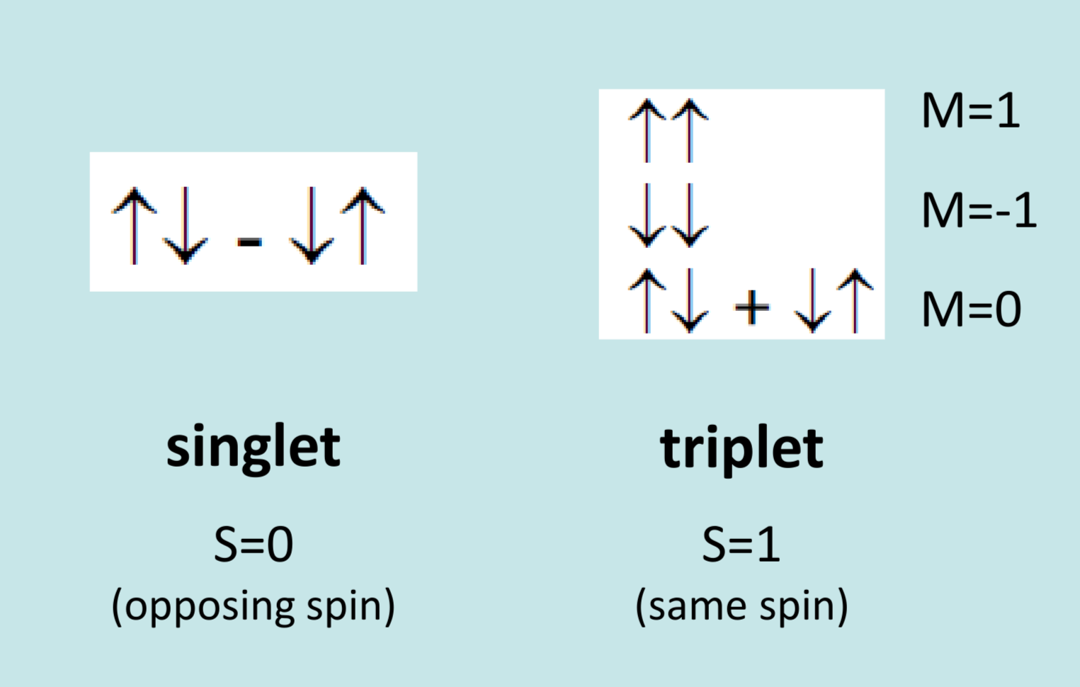
Singlet Triplet Splitting
Singlet state is when two electrons have opposing spin, with a net spin of 0. Triplet state is when two electrons have the same spin state, causing a net spin of +/- 1
There are 3 x the amount of triplets, 3:1 triplet:singlet ratio.
This has applications in many OSC devices
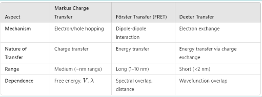
Charge Transfer
Transfer vs Transition: Transfer is between molecules, transition is within the same atom/molecule. Think of Interstate vs Intrastate
3 Types: Forster, Dexter and Markus
Forster Transfer:
- Dipole-Dipole
- Non-radiative
- Swapping
- Requires spectral overlap
- Rate given by:
Where:
- is the rate at which electrons undergo Forster transfer
- , or the experimental photoluminescance lifetime
- is the Forester radius
- is the distance between molecules
Summary:
Dimerization is caused when a material adopts alternating bond patterns. Degree of pi-bond electron delocalization is measured by conjugation length. Longer conjugation = more delocalization = lower LUMO and higher HOMO = smaller band gap and vice versa. Polarons are charged particles that move through and disrupt a lattice structure. Excitons are a bound state of an electron and a hole, that can move a little bit. Polarons can affect a materials optical properties, excitons can recombine to emit light or be separated to generate energy. Singlets and triplets are two types of excitons, singlets have opposite spin and triplets have same spin. Singlets can undergo fast florescence, while triplets undergo slow, sometimes nonradiative, phosphorescence. This is due to Pauli exclusion principle.
Equations:
Where:
- is the number of excited states that decay in a time interval
- is the decay reate
- is the population of excited states
Where
- is the decay rate, composed of radiative and nonradiative decay.
Where
- is the decay through a specific non-radiative channel
Where
- is the decay time of the excited state
- is the time passed
- is the initial population of excited states at
More important equations
Where
- is luminescence
This is the Photoluminescence Quantum Efficiency or PLQY.
Types of OSCs:
Comes in either single molecule or polymer form. Three main uses studied, OLEDs, OPVs, and OFETs.
OLEDS
Organic Light Emitting Diodes.
OLEDS are super cool because they’re simple and can be used to make really good screens.
Two types of control for OLED screens: AMOLED and PMOLED
AMOLED stands for active matrix OLED, and PMOLED for Passive matrix OLED. AMOLED is harder to make but better, faster and more efficient.
Basic structure of an OLED:
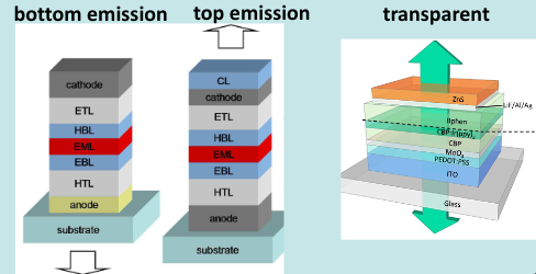
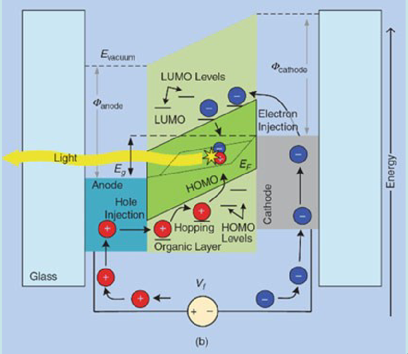
These are, at the most simple level, devices that convert current into light. This is done with the following steps:
- Injection of charges
- Charge Transport
- Exciton formation
- Radiative Recombination
Charactarization of OLEDs
- Driving Voltage
- Luminance
- Driving Current
Where is the current efficiency
Where
- represents the Electroluminescence Quantum Efficiency aka Internal quantum efficiency
- represents the photoluminescence efficiency given by
- represents the ratio of singlet excitons to total excitons
- is the exciton formation factor, defined by
Photoluminescence Efficiency
- Given by equation above
- Represents ratio of radiative to nonradiative recombination of singlets
- Affected by aggregation quenching: The formation of dimers and co-facial aggregates (???) which leads to energy level splitting. In simple terms, puts energy levels between radiative levels, leading to nonradiative decays from singlets. Basically, when molecules clump together and emit heat instead of light
- Can also be affected by optical design, and contaminants
OPVS
Organic Photovoltaics.
Organic semiconductors that turn light into electricity
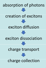
The basic process of a photovoltaic cell involves capturing incoming photons, turning them into excitons, and diffusing the exciton into electrons and holes that can be then collected and turned into usable electricity.
They can be designed in a few different ways, with a bulk heterojunction, in which the photoactive layer is a diffuse combined substance, or a single heterojunction, in which there are two combined layers.
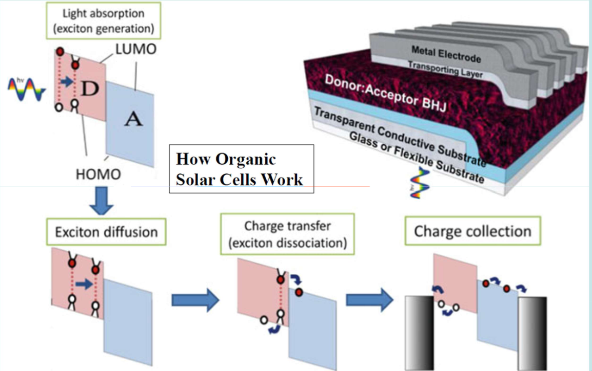
the red “D” is the electron donor, and the blue “A” is the electron acceptor
The diagram top left shows a single heterojunction, and the diagram on the top right shows a bulk heterojunction
Planar/Single heterojunctions are easier to make, but offer worse absorption and longer diffusion lengths between materials. This leads to lower efficiency
Bulk heterojunctions are harder to make, but offer higher absorption and a shorter distance to the interface. However, sometimes you have “islands” of electron donor/acceptor that are not matched to the appropriate electrode
Loss mechanisms occur at several points
- Photons can be reflected or transmitted through the donor and acceptor layers
- Excitons can recombine before being separated
- Charge transport can fail to fully disassociate excitons
- There can be recombination at charge collection and transport phases
The theoretical maximum efficiency for a single junction solar cell is 33.7% at 1.34 eV, but you can go higher with multi-junction cells that have several layers.
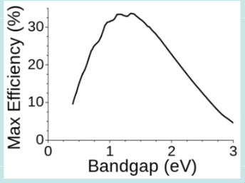
This is known as the Shockley-Queisser limit
Several reasons for this limit:
- Black body radiation
- Recombination of excitons
- Three loss mechanisms: Relaxation, geminate recombination, and non-geminate recombination.
- Geminate recombination is where a previously combined pair recombines, nongeminate is two different pairs recombine with eachother.
- Spectral losses (only photons with energy greater then bandgap are usable)
- Impedance matching (Resistance load must be matched)
Testing condition for solar panels is known as AM1.5, this represents a 48 degree solar angle, or 1.5x the thickness from the atmosphere normal to the ground.
Characterization of OPV cells
JV Curve is an important quantitative metric for photovoltaic devices. It represents a graph of current density versus applied voltage
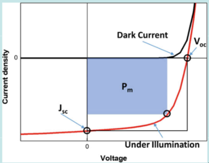
The red line is the JV curve under light, while the black one is the JV curve in the dark.
An important efficiency metric is the fill factor, which represents how “rectangular” the illuminated JV curve is.
The fill factor is given by the following:
Where and are the current density and voltage at maximum power, respectively
This fill factor can be used to calculate the PCE, the power conversion efficiency through the following:
Where:
- is the maximum power point
- is the power of the incident light
- is the fill factor
- and are the short circuit current and open circuit voltage respectively
OFETS
Organic Field Effect Transistor
OFETs are useful for embedded, low performance logic devices such as e-paper, chip cards and RFID tags. They are also used for higher-performance applications as driving stages for flexible AMOLED displays
To understand the OFET, we must first look at the FET, or regular field effect transistor
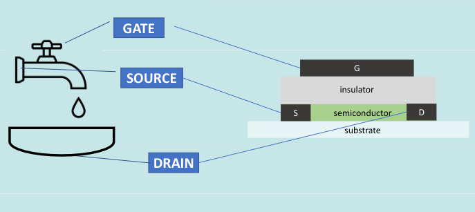
This device deactivates the flow of electrons from the source to the train, until a current is applied to the gate.
OFET’s are the same, but with organic materials instead of silicon or other inorganic semiconductors.
There exists a few different architectures for OFETS:
- Top Gate, bottom contact (Hard to make, good)
- Top gate top contact (Hard to make, Bad)
- Bottom gate, bottom contact (Easy to make, cant be exposed)
- Bottom gate, top contact (Sucks)
Comes in p-type and n-type
- P-type: low gate voltage, power flows when negative/zero voltage applied. Current flows from Drain → source
- N-type: High gate voltage, power flows when high voltage applied. Current flows from source → drain
Characterization equations for OFETS
Two operational modes:
- Linear regime
- Saturation Regime